Welcome to the Thin Films and Microscopy Lab
Our
Laboratory is the result of a collaborative effort between the Department of Physics and Astronomy
and the Department of Biology
.
This laboratory is equipped with a
Digital Instruments Scanning Tunneling Microscope (STM) and Atomic Force
Microscope (AFM) (Nanoscope II System). These instruments are being used for
the study of solid-state materials such as semiconductors, metals and
semimetals and biological molecules such as genomic DNA. The laboratory is also
outfitted with a JEOL-JSM-6100 Scanning
Electron Microscope (SEM) that provides the ability to directly image the
microstructure of solid state and biological samples down to approx. 100nm. The
laboratory possesses the necessary ancillary equipment for SEM of biological
samples such as a critical point drying apparatus and sputter coater. In
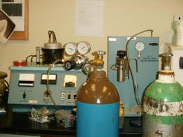
addition, the laboratory is equipped with a rotating disc electrode, an
electrochemical analyzer, and a metallurgical polisher (Buhler Ecomet IV), all
of which are used for growing semiconductor thin films.
Some of the current areas of research include the
fabrication of thin films by electrochemical deposition under potentiostatic or
galvanostatic control. In particular, we are studying the growth and
characterization of multilayered thin films for use in solar cell technology.
Additional projects include the study of genomic DNA molecules by STM and AFM
on various substrates. Undergraduate projects include the development of a
Scanning Probe Microscope system for use in microgravity materials research.
About
the AFM and STM
Binnig, Quate and Gerber
invented the Atomic Force Microscope (AFM), or Scanning Force Microscope (SFM)
in 1986. It is the daughter instrument of the earlier Scanning Tunneling
Microscope (STM), which was invented by Binnig and Rohrer at IBM Research
(Zurich) in the early 1980s.
The STM can image individual lattice sites on the surfaces of conductive or semiconductive crystalline materials. It has made significant contributions to the semiconductor industry and materials science in general. For example, the STM gave the first direct evidence of the 7x7 reconstruction of the silicon <111> surface. Shortly after the invention of the STM, Binnig, Quate and Gerber introduced the Atomic Force Microscope (AFM) in 1986. The AFM can image insulating and conducting surfaces, often with the same resolution as the STM. As a result the AFM has found application in many fields of surface science, nanotechnology, polymer science, semiconductor materials processing, microbiology and cellular biology.
Our
Laboratory is the result of a collaborative effort between the Department of Physics and Astronomy
and the Department of Biology
. The Lab is outfitted with a Digital Instruments AFM that is being used in
various areas of research.
Current Areas of Research
Thin Films
|
|
|
|
Welcome to the Thin Films and Microscopy
Laboratory |
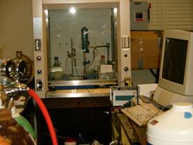
Thin Film Deposition Area: Shown is the Rotating Disc Electrode (RDE)
used to deposit CuInSe2 and CuInS2 thin films. |
|
|
|
|
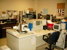
Scanning Electron Microscope Jeol 6100 |
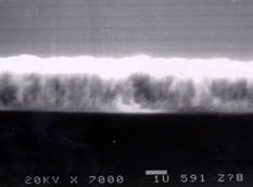
SEM Image of cross-section
of electrodeposited CuInSe2 thin film. |
|
|
|
|
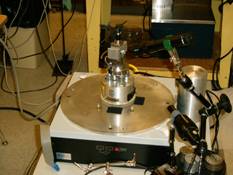
Atomic
Force Microscope & Scanning Tunneling Microscope (Digital Instruments
Nanoscope II) |
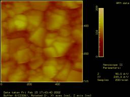
AFM Image of
electrodeposited CuInS2 thin film |
|
|
|
|
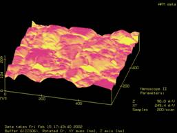
AFM Image of electrodeposited CuInS2
thin film (surface plot) |
Sputter Coater used to coat samples and substrates
with a conductive coating. |
(AFM Images of Carbon Nanotubes on
Graphite Substrate)
Cellulose Fibers
(AFM Images of Cellulose Fibers on Mica
Substrate)
Other sample images from the AFM lab can be found here: Images
A
number of companies make Scanning Probe Microscopes commercially, although it
is also possible to build one yourself. You may visit these sites to find out
more about scanning probe microscopes:
University sites:
Commercial
sites:
Digital Instruments-Atomic Force & Scanning Probe Microscopy
Jeol Scanning Probe Microscopes
Other
Links:
Publications
and Presentations
Scanning Tunneling
Microscopy of Electrodeposited CuInSe2 Nanoscale Mulilayers,"
R.P. Raffaelle, J.G. Mantovani, and R. Friedfeld, Solar Energy Materials and
Solar Cells, 46, 201 (1997).
Electrodeposition of
CuInxGa1-xSe2 Thin Films," R. Friedfeld,
R.P. Raffaelle, and J.G. Mantovani, Solar Energy Materials and Solar Cells
58, 375 (1999).
Electrodeposited CIS-based Solar
Cell Materials", R. Raffaelle, T. Potdevin, J. Mantovani,
R. Friedfeld, S. Bailey,
Materials in Space, pp. 123-128, (1999).
"A Two-Step Electrochemical
Deposition Process for the Fabrication of CIGS Thin Films",
R. Friedfeld, J. Mantovani, R.
Raffaelle, A. Hepp, S. Bailey, Materials in Space, pp. (1999).
Electrodeposited CdS on CIS pn
Junctions", R. Raffaelle, H. Forsell, T. Potdevin, R. Friedfeld,
J. Mantovani, S. Bailey, S.
Hubbard, E. Gordon, and A. Hepp, "Solar Energy Materials and Solar
Cells", 57, pp. 167-178, (1999).
Electrodeposited CIS-based Solar
Cell Materials", R. Raffaelle, T. Potdevin, J. Mantovani,
R. Friedfeld, S. Bailey,
Materials in Space, pp. 123-128, (1999).
Electrodeposited CIS-Based Solar Cell
Materials. R. P. Raffaelle, T. Potdevin, J. G. Mantovani, R. Friedfeld, J.
Gorse, M. Breen, S. G. Bailey, and A. F. Hepp in Materials in Space - Science,
Technology, and Exploration. A. F. Hepp, J. M. Prahl, T. G. Keith, S. G. Bailey,
and J. R. Fowler, Editors; Symposium Proceedings Volume 551, Materials Research
Society: Pittsburgh, pp. 123-128 (1999).
Annealing Effects on
the Self - Assembly of Synthesized Organic Molecules on Au (111) Substrates, Robert Friedfeld, Neil Mulchan, Rolando
Branly, Oladipo Ogunjimi, Steve Scurlock, Herbey Solis, Physical
Society, Annual APS March Meeting 2003, March 3-7, 2003, , abstract #B24.009
03 (2003)
Modeling of CuInSe2
and CuInGaSe2 Superlattices, Scurlock, Steven;
Friedfeld, Robert
Stephen F. Austin
State University, American Physical Society, Annual APS March Meeting
2003, March 3-7,
(2003).
Possible
Applications and Limitations of Multi-Walled Carbon Nanotubes to Solar Energy
Conversion, Robert Friedfeld, Joint Spring
Meeting of the Texas Sections of the APS, AAPT, and Zone 13 SPS March 3–5, 2005; Nacogdoches, TX ( 2003).
“Atomic
force microscopy in zero-g”, Friedfeld, R. Parker, S. Rodgers, G. Meador, R.
Williams, R. Johnson, M., Branly, R.,
Dept. of Phys. & Astronomy, Stephen
F. Austin State University, Nacogdoches, TX, USA, IEEE Aerospace Conference 2003 Proceedings. Page(s): 1- 89
vol.1 ISSN: 1095-323X March 8-15, (2003).
“Atomic
Force Microscopy of Carbon Nanotubes”, Bright
Ideas Conference, Stephen F. Austin State University, (2006)
“Carbon Nanotubes: Production, Purification, and Characterization”, Jonathan Belew, Matt Pusko, Carson Fuls, Robert Friedfeld, Texas Physics Spring 2006 Meeting (2006)